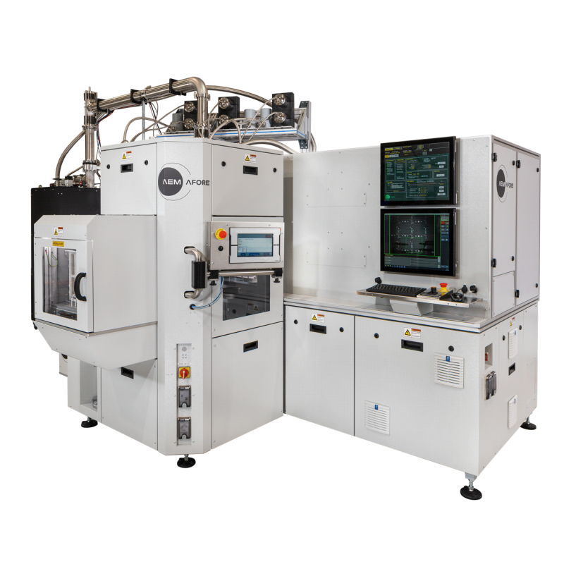
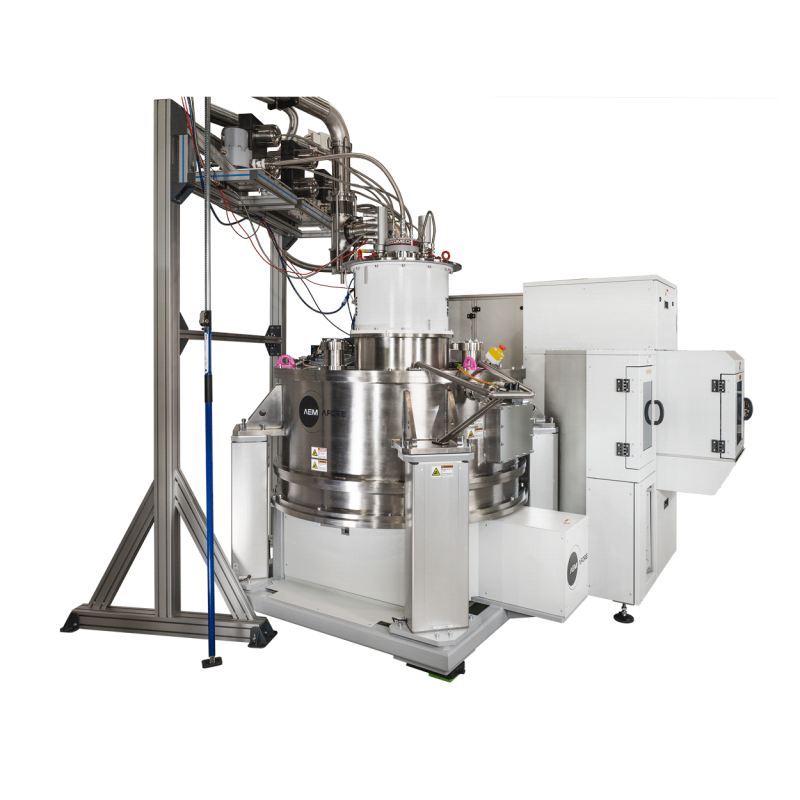
Faster characterization
Sample characterization runs up to 100 times faster than a typical cryogenic chamber, so device, electronics, and detector work moves off a one-at-a-time cooldown.
 H-GATE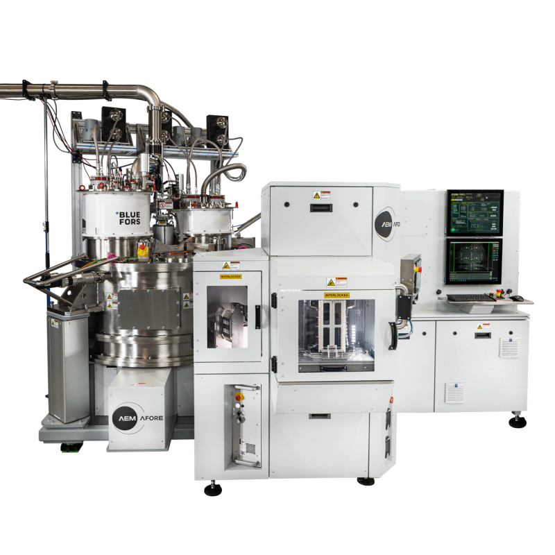
Home / Products / Cryogenic wafer prober
High-throughput characterization
Wafer-level tests for quantum devices, electronics, and detectors. The stage holds 150 mm, 200 mm, and 300 mm wafers, reaches below 2 K at the wafer surface, and can run the load and the measurement without an operator at the chamber.
01
Sample characterization runs up to 100 times faster than a typical cryogenic chamber, so device, electronics, and detector work moves off a one-at-a-time cooldown.
Automatic handling and measurement sit below 2 K, read at the wafer surface. Helium and 4 K cryostat inserts keep that temperature stable and even across the wafer.
Sensors and cameras place and measure the wafer. The cycle can run fully automatic.
The prober uses the same cryogenic lines as the coaxial page: small heat load, low noise, and ratings for repeated thermal cycling.
RF and DC probe cards are built for the measurement instead of a single fixed pinout.
The controller is part of the system. It shows the temperature state and gives direct control without a separate console.
02
Base temperature is read from the surface of the wafer.
| Property | Value |
|---|---|
| Wafer size | 300 mm, 200 mm, and 150 mm |
| Travel | ±160 mm XY, 0–40 mm Z, ±4° theta |
| XY accuracy | ±20 µm |
| Travel speed | Up to 35 mm/s in XY, fully adjustable |
| Wafer base temperature | < 2 K, measured at the wafer surface |
| Wafer exchange | About 3 hours, measurement to measurement |
| Wiring capacity | Up to 768 single DC lines, or up to 48 RF lines at 18 GHz or 40 GHz |
| Wafer loading | From a FOUP or magazine, or by hand into the load lock |
03
A robotic arm loads 150 mm, 200 mm, and 300 mm wafers from a magazine into the load lock. A pre-aligner sets the orientation before the wafer enters the lock, so the system can run without someone at the chamber.
Exchange kits retune the same prober for another diameter. One system can switch between sizes instead of staying on a single wafer format.
A probe card slides into the backplane. The connectors mate as a group, so each RF and DC lead does not have to be plugged by hand.
04
Each install is drawn for its room. Use that drawing for dimensions. The standard arrangement is the nine blocks below.
05
The room needs 3-phase power, cooling water, and compressed air. The longer pre-install list, including flow and electrical detail, is issued with the layout drawing.
Sales